-
Notifications
You must be signed in to change notification settings - Fork 0
dacs
The ocra-pack project uses the ocra hardware: a Red Pitaya/STEMlab, a gradient DAC board, and associated power supplies, amplifiers etc that are unique to each setup.
There are two options for the gradient DAC board:
- the OCRA1, designed by Marcus Prier at Otto von Guericke Universität (OVGU) for their tabletop scanner system (German press release).
- the GPA-FHDO, designed by Benjamin Menkuec at Fachhochschule Dortmund (FHDO) for teaching and research (GitHub page).
See below for information about each board. Both Marcus Prier and Benjamin Menkuec have very kindly made their designs available to the ocra community, and all credit for the designs goes to them.
Currently there are no shared pins between the GPA-FHDO and OCRA1
The OCRA1 and GPA-FHDO serve a similar purpose, but differ in a few major ways; see below. The primary difference is that the GPA-FHDO provides 10A current outputs directly, whereas additional gradient amplifiers are needed for the OCRA1. The OCRA1 provides an RF attenuator. Both boards will provide a Schmitt-triggered output for TR switch control [planned, 23.10.2020].
| Parameter | OCRA1 | GPA-FHDO |
|---|---|---|
| Channels | 4 | 4 |
| Interface | four-channel SPI | single-channel SPI (galvanically isolated) |
| DAC chip | 4x AD5781 | 1x DAC80504 |
| DAC resolution | 18 bits | 16 bits |
| Supply voltages | -15V, +3.3V, +15V | 13-25V (single supply) |
| Outputs (voltage) | +/- 10V single-ended, +/- 20V differential | 0 - 5V single-ended (intermediate) |
| Outputs (current) | - | 4x +/- 10A (integrated power amplifier) |
| Peripherals | PE43704 attenuator, Schmitt trigger for TR switch output | ADC ADS8684 for monitoring and in-sequence calibration |
| Maximum tested speed | ~2 Msps for 4 channels [limited by SPI data integrity] | ~500 ksps for 4 channels [limited by SPI data integrity] |
The OCRA1 provides 4 channels of +/- 10V buffered output at 100 ksps (~50 kHz bandwidth) but can run much faster. There is also an RF PE43704 digital step attenuator, and a digital output with a Schmitt trigger to control an external RF gate.
Each DAC channel consists of an AD5781 serial DAC with a buffered +/- 10V output provided by an AD8675 op-amp. An extra differential output is provided by a THS4131 differential op-amp.

The PCB requires reasonably low-noise +/- 15V supplies for the analog circuitry; other voltages, e.g. 12V-16.5V, should work but have not been tested. A +3.3V supply is required for the digital circuitry. The analog and digital grounds are connected internally in the PCB.
When powering on, ensure the +/- 15V supplies are turned on before the +3.3V, so that the DAC powers on in a known state (see datasheet p24).
The unloaded PCB requires 100 – 150 mA on +15V, a similar amount on -15V, and <100 mA on +3.3V. These increase with load on the outputs. If only one rail is powered, the current draw on the other rail grows by 2x-3x, and the chips can become very hot. During testing, make sure both rails are powered and that you set a current limit of 150 – 200mA on your benchtop power supply. The DAC output buffer chips can also become quite hot when loaded; this is normal behaviour.
[TODO: someone should test current draw with attenuator enabled, loaded current draw]
Each DAC channel has a BNC connector providing the buffered +/- 10V output. An RJ45 connector, J17, provides the same outputs in one place, and a second connector, J18, also provides the differential outputs. Each channel also has a standard 1.26mm pin header from which these can be measured/debugged.
SMA connector J21 is the RF input for the attenuator, and the attenuated RF is output to BNC connector J22.
BNC connector J20 provides the debounced TX gate signal at 3.3V.
The DACs are controlled via SPI from the STEMlab, with shared CLK, SYNC and LE lines, and a dedicated STEMlab-to-DAC data line to each channel.
The DAC readback data lines are unconnected.
The RF attenuator is also serially controlled, with three dedicated lines from the STEMlab.
The digital outputs from the STEMlab can be connected directly to the board’s control lines, or through RC filters to reduce coupling of the digital I/O into the DAC outputs. (In the June 2020 PCBs built by Vlad, the capacitors have been omitted for now.)
[TODO: contact details for Marcus?] Currently the PCB must be manufactured/assembled by individual groups wishing to use it.
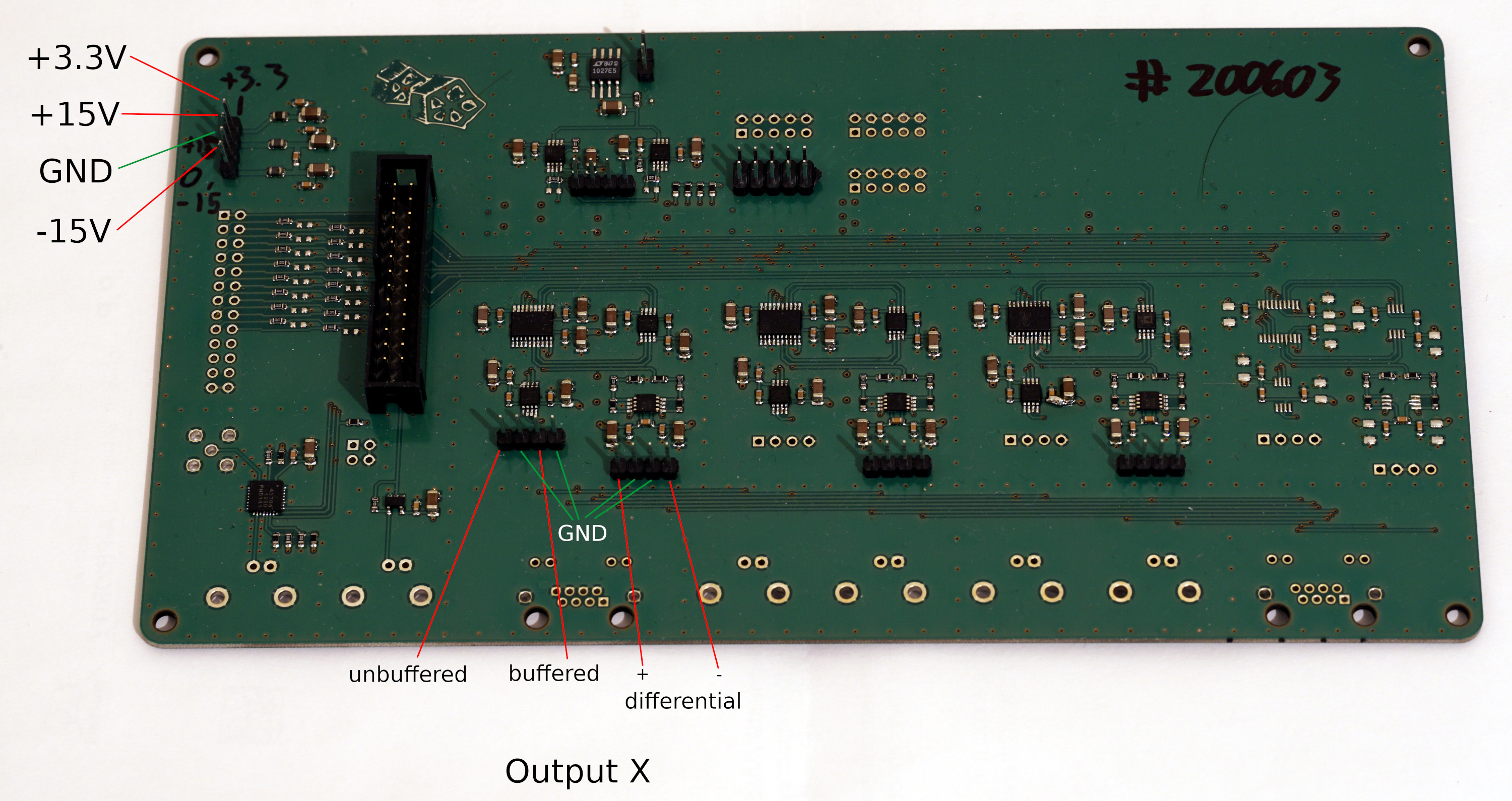
The OCRA1 digital headers are pin-for-pin compatible with the STEMlab’s header. You can connect them using a 13x2 1.26mm-pitch ribbon cable, or using individual jumper wires as shown in the pictures below.


The power connections and DAC outputs for the X channel are shown below. The other channels are the same. The four rightmost BNC connectors are connected to the buffered output of each channel.


A detailed documentation can be found in this wiki.
The SPI interface is a available on a rj45 connector and has the following pinout:
| Pin | Color | Function |
|---|---|---|
| 1 | white/orange | GND |
| 2 | orange | VDD |
| 3 | white/green | GND |
| 4 | blue | CLK |
| 5 | white/blue | GND |
| 6 | green | MO |
| 7 | white/brown | CS |
| 8 | brown | MI |
The abbreviations are: MI (master in), MO (master out), CLK (master clock), CS (chip select). CS low activates the DAC, CS high activates the ADC. VDD can be either 3.3V or 5V depending on the high level of your SPI host-interface.

The power connector is a Molex 0039300100, where pins 3,4,5,9,10 are +VCC and pins 2,6,7,8 are GND
